The Perfect Nanotube
Adsorption experiments are one-time experiments that can not preserve the clean surface of the nanotubes during an experiment. It is also evident that only one nanotube per sample can be observed and studied. Therefore, it is crucial to select the best nanotube for the upcoming adsorption studies. Within the limit of the nano stage, this requires scanning all trenches in this range. Camera images can give great insight into the locations of these tubes. As described by Ishii et al.[136], a subsequent exact scan for the identification of the exact position as well as the identification of aggregates is needed. Such an exact scan reveals the positions of the brightest nanotubes that are then taken to further examinations. For this information, statistical methods are combined with a manual analysis. It is also possible to easily study principal phenomena like defect generation or spectral diffusion in this system which is necessary for adjusting the excitation power to the setup.
Setup
Monochromator
Spectra were taken confocally using an Andor Shamrock 303i-B-SIL monochromator with an integrated grating turret with two gratings of 300lines/mm blazed at 500nm and 1200nm and one grating for high range and lower resolution with 150lines/mm with the blaze wavelength at 1250nm. A typical slit width for the experiments is 200µm. NIR and VIS measurements were performed with an Andor Newton DU920P-OE detector. This detector has 1024x255 pixels with a quadratic pixel size of 26µm, which is an effective diagonal of 28.5mm. The vertical binning was reduced to 25 pixel to remove dark noise and spikes at longer integration times. Spectra from microscopic measurements use an illuminated pixel size of only around 300µm on the detector. Therefore, the detector readout was constrained to a subset of 25 vertical pixels, which essentially covers the total emission area and leaves room for some alignment errors. Selecting a subset of 25 pixels also reduces the RMS noise and reduces cosmic ray spike generation. An Andor iDus model DU491A-1.7 covered the SWIR range with 1024x1 pixels and a pixel size of 25x500µm. The detection area and illumination are comparable to the binned silicon camera and completely cover the spacial extension of the microscopic emission. Both detectors are cooled thermo-electrically to -90℃ with an additional attached water cooling for temperature stabilization.
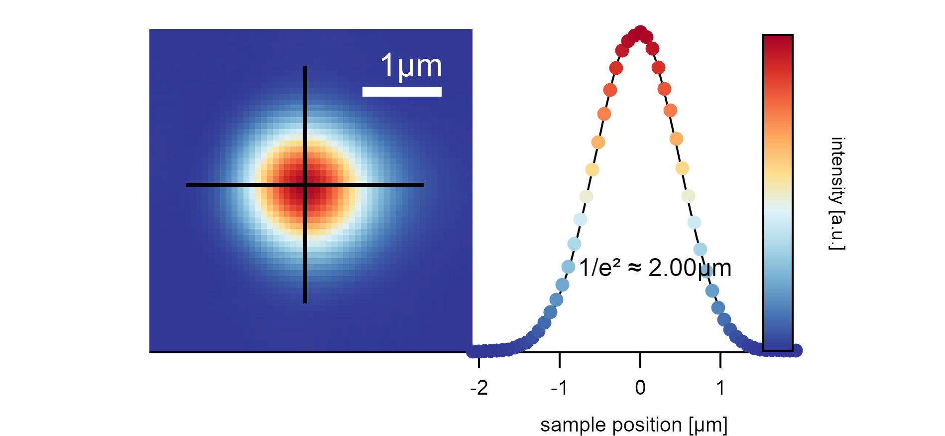
The laser profile of the SuperK after the fiber output is around 1.2mm broad. If focused on the sample with the objective, it illuminates the area with a diameter of 2µm (the diameter of the laser spot is measured where the maximum intensity I₀ drops to I₀/e²).
Excitation in epi geometry was accomplished using a chroma 760nm dichroic mirror and an 830nm color glass long pass filter. For the excitation of the sample area, a NKT SuperK Extreme light source is used, which generates a suitable white light spectrum. A NKT Varia was added for wavelength control of the excitation bandpass. The excitation light is filtered by two NIR neutral density absorption filters and a variable neutral density filter to adjust output power. Laser performance was continuously measured and recorded from the reflection at a thin glass plate using a Thorlabs PM100D power meter.
Excitation
The excitation spectrum of the light source varies with the selected bandpass and emission power. For a bandpass of 550-725nm, the excitation spectrum varies with the output power. Dashed lines indicate the limit of the excitation range due to absorption in the dichroic mirror.
The maximum output of the NKT SuperK in this setup is 18W. The spectrum varies strongly over the visible range and intensifies to the NIR due to the white light generation process using a NIR pump laser. Thus also the excitation power varies depending on the selected bandpass and the pump laser emission strength.[155] The NKT output was fixed to 40%, and the excitation power was then reduced with a variable neutral density filter to reduce the actual power on the sample. The emission control was fixed at 40% during photoluminescence excitation measurements. As the spectral weight varies over the excitation range, the power was continuously measured and used for excitation corrections.
Power
Excitation of a suspended carbon nanotube has to happen below 50µW with a 20nm bandpass that fits the targetted chirality. Continuous shifting of the excitonic emission peak to the blue is a commonly observed phenomenon for measurements in air.
Excitonic emission from carbon nanotubes has shown to be sensitive to the excitation power. The irreversible generation of defects at high power due to the reaction with oxygen leads to the formation of defect sites, which act as exciton trap states leading to a decrease in photoluminescence intensity with an accompanied red-shift of the emission signal. A non-linear, reversible reduction of the intensity is observable above 25µW excitation power. This reduction of the intensity originates from electronic many-body interactions leading to exciton-exciton annihilation. An additional but more critical factor for the following experiments is the subsequent shift of the emission spectrum to higher energies at higher laser powers. The shift originates from changes in the dielectric environment that are caused by a laser-induced temperature increase of the adsorbed molecules. In our setup, a typical individual semiconducting carbon nanotube is excited with a 20nm broad spectrum of 662.5-682.5nm at the excitonic transition in its second electronic subband. In such a system, the nanotube shows energy-stable emission at around 20µW excitation power.
Note
The setup-specific excitation power at the sample is six times higher than the measured reflection at the glass plate. However, the spectra in this work are normalized to the photon flux measured at the glass plate as the ratio is proportional.
Polarization
The emission output after the NKT Varia is elliptically polarized. Carbon Nanotubes are excited to their E₂₂ states only if the excitation aligns with the nanotube elongation axis. Although there are states like the E₁₂ or coupled phononic states that can be excited perpendicular to the axis. The absorbance of these states is generally lower, which in turn also gives lower emission when relaxed to the E₁₁ level. Thus, carbon nanotubes can theoretically be excited in every polarisation direction. However, to ensure that the maximally possible spectral overlap is happening, the emission for different polarisations was tested. In all measurements, the nanotube emission maximum coincides with the maximum of the NKT excitation. Most homogeneous polarisation measurements, though, were performed with an angle offset of around 25° to the elliptical laser excitation axis which suggests that there is some degree of skew between the orientation of the nano stage and the polarisation of the light source that is most probably due to the alignment of the uplift mirrors. In short, polarisation is not expected to have a significant impact on this setup with a high tolerance of ±30° to the nanotube axis.
Spectral Window
The as-described setup is limited when taking spectra above 1300nm due to the absorption of the dichroic mirror. It excels, on the other hand, at taking spectra between 830nm and 1000nm. It allows observation of carbon nanotubes with diameters from 0.7nm to 1.2nm, which is also the targeted diameter of the chemical vapor deposition synthesis. Even though at 800℃, most carbon nanotubes emit between 1100 and 1200nm, the nanotubes that emit between 800 and 1000nm show excellent emission properties, which are most probably due to their high photoluminescence quantum yield estimated to around 7% [156].
The blue spectra were measured using a silicon detector, the red spectra using an InGaAs detector. The dotted line shows the quantum efficiency for the detectors. The measurement range is limited at low wavelength by an 830nm long-pass filter and at high wavelength by the absorption of the chroma 760nm dichroic mirror.
Also, gratings need to get considered when taking spectra. Gratings distort the
spectrum nearly quadratically to the edges as each grating is optimized for a
specific Blaze wavelength. These effects are reduced computationally with
grating correction curves. Additionally, if the spectral intensity among
gratings with different amounts of lines per mm needs to get compared, the
intensity can be corrected to the wavelength pitch [cts/nm] but
stats.booWavelengthPitch as such a correction alters integration results.
When acquiring wavelength-dependent spectral information, the spectra are
furthermore corrected to the quantum efficiency curves of the detectors. The
measured excitation power is then transferred into a photon flux [photons/s] by
taking the central excitation wavelength of the selected bandpass as photon
energy. The microscope setup has a reasonably unusual beam splitter for taking
spectra (Chroma Technology T760LPXR). Due to its varying reflectivity between
500-570nm and setup constraints, it is necessary also to correct the measured
excitation power in this range. All microscopy spectra are furthermore
corrected using the transmission curves of the mounted high pass filters. For
spectra, it is a 750nm (Thorlabs FELH0750) or an 830nm color glass filter. The
filter curves are slightly corrected by the reflectivity of the used silver
mirrors at 45° incidence. Missing data points within these curves are linearly
interpolated. For image acquisition, only the color glass filter mentioned
above was used, and only magnification and tilt corrections are performed
computationally. Spectra with different excitation times were compared, by
normalizing to their exposure time in seconds. All corrections are calculated
using PLEMd2BuildMaps() which preserves the original measurement data
and allows to reversible apply specific corrections. When displaying PLE maps
as images, the pixels are displayed evenly spaced for convenience reasons,
whereas calculation and analysis are always performed on the physically
correct, distorted scale. A measurement series on one nanotube was usually
performed without changing filters, grating, or detectors during the
measurement.
When analyzing multiple camera images in one image, camera images were rotated to match the setup specific rotational offset between nano stage axes and camera pixel alignment. Magnification is corrected for Nikon geometry with an additional constant factor to achieve maximum image overlap for images taken at different positions of the nano stage. The relative positioning of the nano stage within 300µmx300µm is taken as a reference for the magnification correction.
Technique
Trench Scan
A complete raster scan with 2x4µm spacing over 100x100µm with the silicon detector. The circle size indicates the maximum intensity of the spectral emission, and colors indicate the central emission wavelength of the excitonic signal.
The silicon substrate consists of 2µm wide and 3µm deep trenches, evenly spaced in parallel arrangements every 4µm. The center of the laser excitation is positioned on a known offset to the first trench on the substrate. Such zeroing allows performing a scan over all trenches to identify the exact position of nanotubes. The trenches are scanned in 2µm steps along the trench as the laser spot size determines the step size. In such a scan, the rough locations of suspended nanotubes can be estimated. Using a broad excitation of 550-725nm, it is also possible to cover a wide range of chiralities. The downside of this approach is the enormously long scanning time per detector. An area of 100µmx100µm requires 1326 spectra to be taken. Depending on the exposure time per spectrum, which is typically 15s, such a scan can take 5.5h for one detector only. Scanning a sample area of 300µmx300µm with the same exposure time using two detectors would, therefore, require measurements over more than four days and can only identify a fraction of the sample.
Image Scan
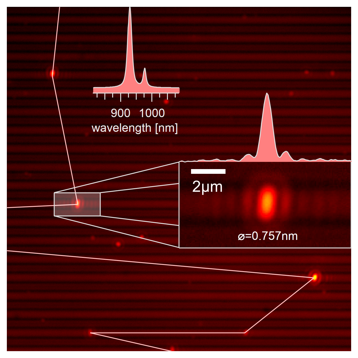
The image is the base information on which a trench scan with rough nanotube positions is performed. The exact positions of the nanotubes are identified with a scan around the position from the image.
Given that the acquired positions always require an additional scan to determine their exact position, only the intensity of the acquired spectrum contains valuable information for the initial scan. An image can give similar information within a smaller time domain and with the use of fewer resources. Images also have the advantage of identifying suspended nanotubes easier as their distinctive emission is homogeneously distributed over the pit. At 660nm, excitation with the 660nm dichroitic beam splitter also attached a characteristic airy stick Bessel function pattern is visible along the axis. The periodicity of the Bessel function can also be exploited for better identification of suspended carbon nanotubes in a large picture when applying a Wigner distribution to separate the phase space pattern along the trench. The maximum visible intensity of theses images also correlates with the spectral maximum of the excitonic emissions when taking spectra at these locations. Images are, therefore, always a must when identifying suspended carbon nanotubes and should be taken first to minimize processing times.
Exact Scan
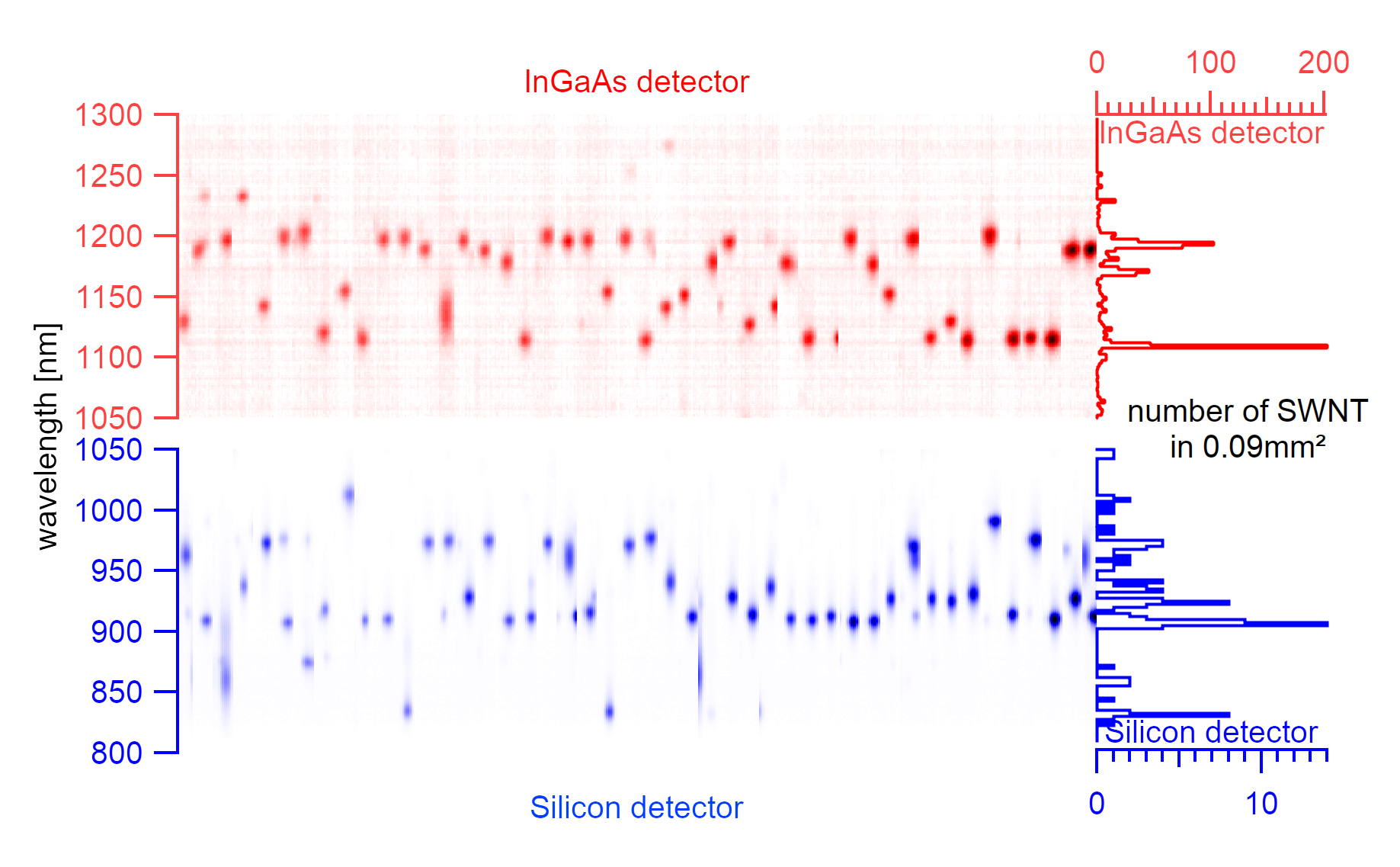
The exact scan technique is a scan along the trench. Eleven spectra are taken around a rough position with the goal of identifying the exact location of the single-wall carbon nanotube from the image. The scan in this image is ordered by the intensity with features of the highest intensity located on the right side.
After finding the rough position of a carbon nanotube, 11 spectra around that position are taken with 0.25µm spacing, and the rough position centered using a broad excitation from 550 to 725nm. It has to be mentioned that the z position for these coordinates can be calculated from the already measured tilt plane. Each of the acquired spectra is manually analyzed to determine the exact position of the nanotubes within 0.25µm accuracy. The fairly narrow excitonic emission spectrum from the E₁₁ state also allows for rough identification of the chirality.
Overall smaller peak areas are accomplished with the InGaAs detector if the spectra are normalized to the exposure time. The detection area for both detectors is roughly the same, and the quantum efficiency within the measured range is generally higher by one order of magnitude for the InGaAs detector. Thermal (Johnson) noise and low signal digitization lead to these general culprits of the InGaAs detector.
Most carbon nanotubes have their emission in the SWIR range, but although the number of visible nanotubes in this range is higher, their peak area is generally also smaller by three orders of magnitude. The peak area was measured on the wavelength axis and is expected to be even more on the energy axis. The adsorption measurements in solution are sensitive to emission drops and require a high resolution of the nanotube emission intensity. Considering the inferior emission properties in the SWIR range, only nanotubes from the NIR range were used for adsorption measurements.
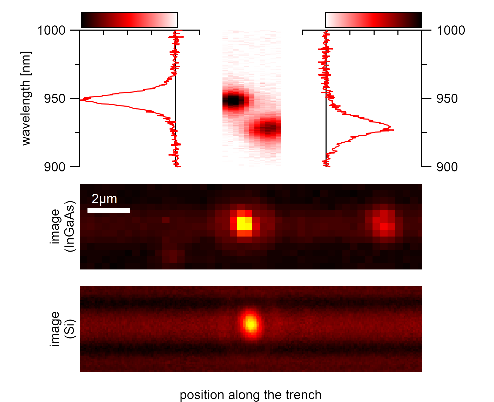
Two nanotubes that seem like a hetero aggregate when taking image and spectrum at their mean position. Using the exact scan technique, it becomes evident that these nanotubes are the (9,1) type at the right and the (8,3) type in vicinity emitting at a similar wavelength.
The spatially resolved acquisition of spectra allows differentiating between the emission from bundled and unbundled nanotubes locally. Even though the spectrum from the position that was determined by the camera images can show two excitonic peaks, this does not necessarily mean that these nanotubes are bundled. The resolution limit of the light microscopy is simply not enough to clearly differentiate the two emissions, and their spectra merge and overlap to a combined emitter. The spacial information also identifies carbon nanotubes of the same type that are in close vicinity to each other, which is not visible from the pure spectrum but can significantly disturb single molecular spectroscopy as any resulting adsorption measurement would include the combined emission from two nanotubes. Nanotubes located in close vicinity (<2µm) to the same and other chiralities are typically excluded from further analysis.
Analysis
The chiral assignment of a single spectrum is nearly impossible and often leads to mistakes. A wide range of publications have reported chiralities differently which is why today mostly statistical analyses are performed for single molecule measurements. If not done on a comparative base to other single spectra, the interpretation about the diameter is vague. Not differentiating between nanotubes suspended in air and nanotubes in vacuum has been found to be the most prominent mistake that is handled in its own chapter. As shown in the following graph, these mistakes can not be avoided using photoluminescence-excitation spectroscopy solely.
A peak fit shows that the photoluminescence reaches a maximum for specific excitations. These positions originate from different chiralities. Their distinct assignment needs further elaboration.
The selections of best spectra and best PLE maps are available online.
A red-shift of the signal can either be allocated to defect generation [157], the dielectric screening of bundled nanotubes [158] or to a change in the outer dielectric environment [159].
The graph above shows a collection of best measuerements. All are of best quality from an extracted dataset and considered mostly unbundled. The measurements show an inhomogenious set of nanotubes with certain statistical evident peaks in the clustering. K-means clustering should be performed here so the fitting routine needs to be improved to better match the maximum PLE intensity but a grouping into distinct spots is visible. I want to address the reason for this inhomogeniousity in more detail here and in the next chapter. The formation of bundles during a measurement can be neglected and the concentration of nanotubes on the sample was helt low to minimize intrinsic bundling.
As intrinsic bundling as the effect of emission quenching can be excluded here, I want to discuss defect generation in this chapter which is an inherent problem in these measurements. Time-dependent measurements of the photoluminescence from one suspended nanotube on the sample have already shown different effects. Suspended nanotubes are known to undergo irreversible blinking due to photoinduced oxidation [147] upon laser irradiation. This generally also broadens the collective excitonic emission due to a mixing of local defective states with lower energies. At laser powers of 70µW on the sample, the emission intensity rapidly but continuously diminished. The bleaching is accompanied by a correlated red-shift of the emission energy and broadening of the FWHM. Strong r values support this finding. A statistical analysis of the involved peak features can, therefore, help to find a sufficiently low excitation power that avoids irreversible defect formation. In the following chapter in air, the power on the sample was kept below 10µW (laser spot 2µm). These samples show a reversible effect in energy and bleaching that is addressed in more detail in the following chapter.
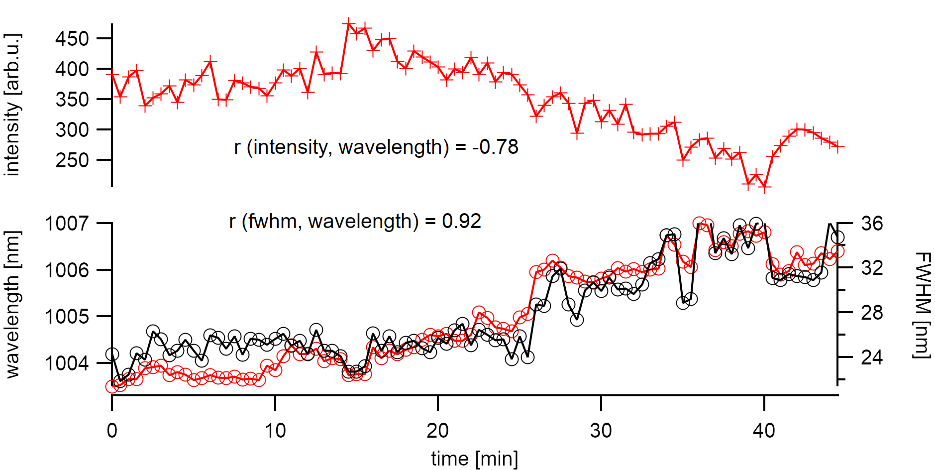
Bleaching of the photoluminescence at 70µW laser excitation strongly correlates with peak broadening and a shift to lower energy. The bleach happens on a rather rapid time scale with a half-life decay of τ=10min.
The emission energy of a carbon nanotube is not stable in energy over time when observed at low exposure times. This behavior is more widely known for low-temperature measurements [13] where excitons are better localized. However, it has also been shown to apply for room temperature measurements.[136] Bleaching is continuous emission depleaching with strongly correlated broadening of the FWHM at high excitations. Bleaching is usually considered irrreversible. In some samples, it is evident that the emission wavelength and FWHM are not anti-correlated with the intensity. This especially occurs at low excitation powers. The discussion of these effects and their impact on the measured spectral distribution will be the topic of the next chapter. Knowing about these changes to the emission energy will also help to assign specific chiralities.
The exact scan technique allows us to fully characterize, a sample area of 300µmx300µm in a short amount of time. The found locations of these nanotubes are the base for further analysis using subsequent experiments where only a fraction of these nanotubes will survive, and their emission strength is significantly reduced.
Nevertheless, recent investigations demand that measurements like the ones present in this study need to be carried out under a protective gas environment. Such changes in the setup design allow to increase the excitation power and thus the emission intensity and reset the system to a save desorbed state without bleaching.
Conclusion
The “exact scan” [136] is an essential technique for finding suspended nanotubes. With the performed alteration, mostly automated analysis of a single sample becomes feasible, which is only limited by the range of the nano stage. Such extensive analyses usually take long time scales to perform. The suggested method yields better results within a smaller time frame giving access to a large pool of suspended nanotubes. Only nanotubes with the most vigorous emission intensity and best camera images from this selection are chirally identified using photoluminescence excitation maps and used for further investigations.
As the emission intensity is significantly reduced in solvents, and it is also crucial to reduce the excitation power, such experiments are only possible with The Perfect Nanotube. The definition of a perfect nanotube can be that it is of a pristine surface, which is discussed in the next chapter. A perfect nanotube may also be a tube that can survive destructive methods such as the ambitious wetting process in the chapter following. The here described method is crucial for selecting the carbon nanotubes that are suitable for carrying out experiments on.